Product Information
When failure is not an option, trust the foundation: PRSE Rigid PCBs. We engineer exceptionally robust circuit boards to be the unwavering core of your most critical devices. By merging superior materials with precision manufacturing, we deliver solutions built for maximum endurance and streamlined production.
From simple single layer to complex high-density designs, our rigid boards provide a cost-effective, resilient, and dependable foundation for the world's vital electronic systems.
| Stack-up | 20L 3LAM |
|
| Final Thickness | 4.4±0.35mm | |
| Plating Aspect Ratio | 12.68:1 | |
| Minimum Hole Size | 0.35mm | |
| Minimum line width/line spacing | 8.0/8.97mil | |
| Surface Finish | ENIG | |
| Inner Layer Copper Thickness | 4oz(78oz Total Cumulative Copper) | |
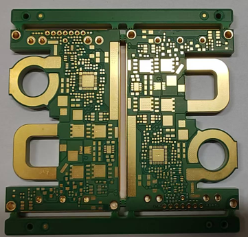
| Business Segment | Server Power Supply |

| Stack-up | 30L 3LAM 2 burried |
|
| Final Thickness | 4.60+/-0.15mm | |
| Plating Aspect Ratio | 15.2:1 | |
| Minimum Hole Size | Micro: 0.1mm, Through: 0.3mm | |
| Minimum line width/line spacing | 5.91/7.87mil | |
| Surface Finish | ENIG | |
| Inner Layer Copper Thickness | 3oz(75ozTotal Cumulative Copper) | |
| Business Segment | Server Power Supply |

| Stack-up | 14L 1LAM |
|
| Final Thickness | 1.6±0.16mm | |
| Plating Aspect Ratio | 5.88:1 | |
| Minimum Hole Size | 0.25mm | |
| Minimum line width/line spacing | 4.5/7.41mil | |
| Surface Finish | ENIG | |
| Impedance Controlled PCB | 14 Impedance Control Lines | |
| Business Segment | Automotive Domain Control Board |

| Stack-up | 4L 1LAM |
|
| Final Thickness | 1.6±0.16mm | |
| Plating Aspect Ratio | 5.96:1 | |
| Minimum Hole Size | 0.25mm | |
| Minimum line width/line spacing | 6.0/3.72mil | |
| Surface Finish | ENIG | |
| GAP Size | 70±30um | |
| Business Segment | Car LED screen |

| Stack-up | 30 layers, 3 lamination cycles, 2 sequential lamination step |
|
| Final Thickness | 4.60+/-0.15mm | |
| Electroplating Aspect Ratio | 15.2:1 | |
| Minimum line width/line spacing | 5.91/7.87mil | |
| Mnimum aperture size | Blind holes: 0.1mm, Through holes: 0.3mm | |
| Surface Finish | ENIG | |
| Inner layer copper thickness | 3 oz (total copper thickness 75 oz) | |
| Business Segment | AI server power supply |

| Stack-up | 8 layers, 1 lamination cycle |
|
| Final Thickness | 1.6±0.16mm | |
| Electroplating Aspect Ratio | 7.3:1 | |
| Minimum Hole Size | 0.25 | |
| Minimum line width/line spacing | 3.0/3.6mil | |
| Impedance Controlled PCB | 17 Impedance Control Lines on Inner/Outer Layer with 20%-80% Bandwidth Control | |
| Surface Finish | OSP | |
| Business Segment | High Speed & High Frequency AI server power supply |

| Stack-up | 38L, 4LAM |
|
| Final Thickness | 7.0±0.5mm | |
| Electroplating Aspect Ratio | 14:1 | |
| Minimum Hole Size | 0.5 | |
| Minimum line width/line spacing | 4/4mil | |
| Surface Finish | flash gold+hard gold | |
| Business Segment | IC Package Test Board |

| Stack-up | 28L , 3LAM |
|
| Final Thickness | 5.5±0.5mm | |
| Electroplating Aspect Ratio | 15.7:1 | |
| Minimum Hole Size | 0.35 | |
| Minimum line width/line spacing | 3.8/4mil | |
| Surface Finish | EPENIG+ | |
| Business Segment | IC Package Test Board |

| Stack-up | 16L 1LAM |
|
| Final Thickness | 3.5±0.3mm | |
| Electroplating Aspect Ratio | 9.4:1 | |
| Minimum Hole Size | 0.304mm | |
| Minimum line width/line spacing | 6.0/6.6mil | |
| Surface Finish | ENIG | |
| Inner Layer Copper Thickness | 56oz | |
| Business Segment | DC-DC Secondary Power Supply |

| Stack-up | 6L 1LAM |
|
| Final Thickness | 1.7±0.15mm | |
| Minimum Hole Size | 1.5mm | |
| Surface Finish | ENIG | |
| Inner Layer Copper Thickness | 1.2±0.05mm | |
| Business Segment | Planar Transformer |
